Why pH matters in a semiconductor manufacturing system?
pH matters in semiconductor manufacturing systems because it directly affects wafer surface chemistry, wet etching precision, chemical mechanical planarization (CMP) performance, ultrapure water (UPW) quality, particle contamination control, photoresist processing, electroplating stability, corrosion prevention, defect reduction, chemical selectivity, wastewater neutralization, and overall semiconductor device yield at nanometer-scale fabrication tolerances.
- Wafer surface chemistry control: Proper pH maintains stable chemical reactions on silicon wafer surfaces during cleaning, etching, oxidation, and deposition processes.
- Wet etching precision: Acidic and alkaline etchants require tightly controlled pH ranges to achieve accurate etch rates, profile control, and material selectivity.
- Chemical mechanical planarization (CMP) performance: CMP slurry pH directly affects polishing rate, abrasive stability, surface smoothness, and defect generation during wafer planarization.
- Ultrapure water (UPW) quality: Stable pH helps maintain ultra-low ionic contamination levels and prevents unwanted chemical reactions in rinse and cleaning systems.
- Particle contamination control: Incorrect pH can destabilize particles and colloids, increasing particle adhesion and wafer surface contamination.
- Photoresist process stability: pH influences developer chemistry, resist dissolution behavior, and critical dimension (CD) control in photolithography processes.
- Electroplating chemistry stability: Copper and metal plating baths require controlled pH to maintain deposition uniformity, conductivity, and surface quality.
- Corrosion prevention: Proper pH minimizes corrosion of stainless steel piping, quartz systems, process tools, and chemical delivery equipment.
- Chemical selectivity optimization: Controlled pH ensures specific materials react at predictable rates while protecting adjacent wafer structures.
- Defect reduction: Stable pH reduces surface staining, oxide defects, micro-pitting, residue formation, and process-induced wafer damage.
- Process repeatability and yield control: Tight pH control improves batch-to-batch consistency and supports stable semiconductor manufacturing yield.
- Wastewater neutralization and compliance: Semiconductor effluent streams containing acids, alkalis, solvents, and metals must typically remain within discharge limits such as pH 6.0–9.0 before disposal.
- Equipment reliability and maintenance reduction: Correct pH reduces scaling, chemical attack, residue buildup, and premature degradation in fluid handling systems and process tools.
How does pH influence semiconductor manufacturing system quality and safety?
pH influences semiconductor manufacturing system quality and safety because hydrogen ion (H⁺) concentration directly controls chemical reaction rates, material selectivity, surface charge behavior, particle stability, metal ion solubility, corrosion activity, and wafer surface chemistry during highly sensitive semiconductor fabrication processes. Maintaining tightly controlled pH conditions—such as approximately pH 2–5 for acidic etching baths, pH 8–11 for alkaline cleaning solutions, near-neutral pH for ultrapure water systems, and pH 6.0–9.0 for wastewater discharge—is essential to achieve stable wafer processing, minimize defects and contamination, protect equipment, maintain operator safety, and ensure environmental compliance in advanced semiconductor manufacturing facilities.
| Influence Area | Process Factor | Related Terms | Typical pH Value / Range | Impact on Quality | Impact on Safety |
| Wafer Cleaning Efficiency | Surface contamination removal | RCA clean, UPW rinse | pH 8–11 alkaline cleaning | Improves particle and organic removal | Reduces chemical residue accumulation |
| Wet Etching Precision | Chemical etch rate control | HF, acidic etchants | pH 2–5 acidic chemistry | Maintains accurate material removal | Prevents over-etching and chemical instability |
| CMP Slurry Stability | Polishing chemistry control | CMP slurry, abrasive dispersion | pH 7–11 typical | Improves wafer planarization uniformity | Reduces slurry instability and defect formation |
| Photoresist Development | Resist dissolution behavior | TMAH developer chemistry | Highly alkaline conditions | Improves critical dimension control | Reduces lithography defects |
| Ultrapure Water Quality | Low ionic contamination control | 18.2 MΩ·cm resistivity | Near neutral pH | Maintains ultra-clean wafer surfaces | Prevents unwanted chemical reactions |
| Electroplating Stability | Metal deposition chemistry | Copper plating baths | Controlled acidic range | Improves deposition uniformity | Prevents unstable plating reactions |
| Particle Stability Control | Colloidal suspension behavior | Zeta potential, particle dispersion | Process-specific ranges | Minimizes particle adhesion defects | Prevents slurry agglomeration |
| Corrosion Prevention | Equipment material protection | Stainless steel, quartz systems | Controlled chemical compatibility range | Protects process tool integrity | Reduces chemical leakage risk |
| Defect Reduction | Surface quality management | Micro-pitting, staining, residue | Stable process chemistry | Improves semiconductor yield | Reduces process instability |
| Wastewater Neutralization | Effluent treatment systems | Acid and alkali neutralization | pH 6.0–9.0 | Ensures compliant wastewater discharge | Protects environment and facility safety |
Why is the semiconductor manufacturing system sensitive to pH deviations?
Semiconductor manufacturing systems are extremely sensitive to pH deviations because semiconductor fabrication processes operate at nanometer-scale tolerances where even very small chemical imbalances can alter etch rates, wafer surface charge behavior, particle stability, slurry performance, metal ion solubility, oxide formation, and chemical selectivity during cleaning, etching, CMP, lithography, electroplating, and ultrapure water (UPW) processing. Small deviations outside tightly controlled process windows—such as acidic etching baths typically around pH 2–5, alkaline cleaning solutions around pH 8–11, CMP slurry chemistry near process-specific neutral or alkaline ranges, and near-neutral ultrapure water systems with resistivity close to 18.2 MΩ·cm—can rapidly change reaction kinetics and surface chemistry, leading to process instability and yield loss.
If pH becomes too low, excessive acidity can increase silicon, oxide, or metal etch rates, damage photoresist layers, corrode stainless steel and quartz process components, destabilize plating baths, and increase dissolved metal contamination that causes wafer defects and electrical failures. If pH becomes too high, alkaline conditions can cause excessive oxide attack, slurry agglomeration, particle adhesion, chemical precipitation, surface staining, and CMP instability, while also reducing chemical selectivity and damaging sensitive wafer structures. Incorrect pH additionally destabilizes ultrapure water chemistry, increases ionic contamination, alters zeta potential and particle dispersion behavior, reduces cleaning efficiency, and may create wastewater neutralization and environmental compliance problems if discharge streams move outside typical regulatory ranges such as pH 6.0–9.0.
Typical pH ranges and control targets in the semiconductor manufacturing system
Typical pH ranges and control targets in semiconductor manufacturing systems are defined by the chemistry requirements of wafer cleaning, wet etching, chemical mechanical planarization (CMP), electroplating, ultrapure water (UPW) production, photoresist development, chemical delivery systems, and wastewater neutralization processes, where precise hydrogen ion balance is essential to maintain reaction selectivity, surface cleanliness, particle stability, defect control, and process repeatability at nanometer-scale fabrication tolerances. These targets—commonly including approximately pH 2–5 for acidic etching solutions, pH 8–11 for alkaline cleaning chemistries, near-neutral pH in ultrapure water systems with resistivity near 18.2 MΩ·cm, and pH 6.0–9.0 for wastewater discharge—are established based on factors such as material compatibility, etch rate control, slurry stability, zeta potential behavior, ionic contamination limits, chemical selectivity, corrosion prevention, and environmental compliance requirements.
Common pH ranges in semiconductor manufacturing system applications
Common pH ranges in semiconductor manufacturing system applications typically include approximately pH 2–5 for acidic wet etching processes, pH 8–11 for alkaline wafer cleaning solutions, pH 7–11 for CMP slurry systems, near-neutral pH for ultrapure water (UPW) systems, controlled acidic ranges for electroplating baths, and pH 6.0–9.0 for wastewater neutralization and discharge. These ranges are carefully controlled because semiconductor fabrication processes operate at nanometer-scale tolerances where small pH changes can alter etch rates, particle dispersion, chemical selectivity, wafer surface charge, metal ion solubility, slurry stability, contamination levels, and defect formation, directly affecting process yield and device reliability.
| Application / System | Typical pH Range | Process Type | Related Terms | Purpose of pH Control | Risk if Out of Range |
| Acidic Wet Etching Systems | pH 2–5 | Chemical material removal | HF, HCl, acidic etchants | Control etch rate and material selectivity | Over-etching, surface damage, process instability |
| Alkaline Wafer Cleaning Systems | pH 8–11 | Wafer surface cleaning | RCA clean, ammonium hydroxide | Remove particles and organic contamination | Poor cleaning efficiency and residue formation |
| CMP Slurry Systems | pH 7–11 | Chemical mechanical planarization | Slurry chemistry, abrasives | Maintain polishing stability and defect control | Slurry agglomeration and wafer scratching |
| Photoresist Developer Systems | Highly alkaline | Photolithography processing | TMAH developer chemistry | Control resist dissolution behavior | Critical dimension variation and lithography defects |
| Ultrapure Water (UPW) Systems | Near neutral | High-purity rinse and cleaning | 18.2 MΩ·cm resistivity | Minimize ionic contamination | Particle contamination and surface defects |
| Copper Electroplating Baths | Acidic controlled range | Metal deposition processing | Copper sulfate plating chemistry | Maintain deposition uniformity | Uneven plating and conductivity defects |
| Oxide Cleaning Systems | pH 2–4 | Oxide removal processing | Buffered oxide etch (BOE) | Remove oxide layers selectively | Excess oxide loss and wafer damage |
| Silicon Surface Conditioning | Process-specific controlled range | Surface preparation | Surface activation chemistry | Optimize surface chemistry stability | Poor film adhesion and contamination |
| Chemical Delivery Systems | Application-specific range | Bulk chemical handling | Chemical compatibility control | Prevent corrosion and precipitation | Piping damage and chemical instability |
| Wastewater Neutralization Systems | pH 6.0–9.0 | Effluent treatment | Acid and alkali neutralization | Meet environmental discharge regulations | Compliance violations and environmental risk |
Factors that define pH control targets
pH control targets in semiconductor manufacturing systems are defined by wafer material compatibility, process chemistry requirements, etch rate control, chemical selectivity, particle stability, slurry performance, ultrapure water (UPW) quality, metal ion solubility, photoresist behavior, electroplating chemistry, contamination sensitivity, corrosion prevention, temperature stability, wastewater discharge regulations, and semiconductor yield requirements. These factors determine the optimal hydrogen ion (H⁺) balance needed to maintain nanometer-scale process precision, stable surface chemistry, low defect density, high process repeatability, and reliable semiconductor device performance throughout fabrication and cleaning operations.
- Wafer material compatibility: Silicon, silicon dioxide, copper, aluminum, tungsten, and low-k dielectric materials each require specific pH conditions to prevent unwanted surface damage or corrosion.
- Process chemistry requirements: Different semiconductor processes such as wet etching, CMP, cleaning, and electroplating rely on tightly controlled chemical reaction environments.
- Etch rate control: pH directly affects how quickly acidic or alkaline chemistries remove target materials during wafer etching operations.
- Chemical selectivity: Controlled pH allows specific materials to react while protecting surrounding structures and adjacent layers.
- Particle stability and dispersion: pH influences zeta potential and colloidal stability, affecting particle suspension behavior and contamination risk.
- CMP slurry performance: Slurry pH controls abrasive stability, polishing rate, defect formation, and wafer planarization consistency.
- Ultrapure water (UPW) quality: Near-neutral pH helps maintain extremely low ionic contamination levels and resistivity near 18.2 MΩ·cm.
- Metal ion solubility: pH affects dissolved metal contamination behavior, precipitation, and electrochemical reactions within process chemistries.
- Photoresist process behavior: Developer chemistry pH controls resist dissolution rate and critical dimension (CD) accuracy during lithography.
- Electroplating chemistry stability: Copper and other plating baths require stable pH to maintain uniform deposition and conductivity performance.
- Contamination sensitivity: Semiconductor fabrication environments are highly sensitive to trace ionic and particulate contamination caused by unstable chemistry.
- Corrosion prevention: Proper pH minimizes corrosion of stainless steel piping, quartz systems, chemical tanks, and process tools.
- Temperature stability: Process temperature changes alter chemical equilibrium and pH-dependent reaction kinetics during fabrication.
- Wastewater discharge regulations: Semiconductor wastewater streams typically must remain within pH 6.0–9.0 before environmental discharge.
- Semiconductor yield and defect control: Tight pH control reduces micro-defects, residue formation, wafer damage, and process variation, improving production yield and device reliability.
What happens when pH is out of range in a semiconductor manufacturing system?
When pH is out of range in semiconductor manufacturing systems, it can cause incorrect etch rates, wafer surface damage, particle agglomeration, CMP instability, photoresist defects, electroplating non-uniformity, metal contamination, corrosion of process equipment, ultrapure water instability, residue formation, poor film adhesion, micro-defects, yield loss, and wastewater non-compliance because hydrogen ion (H⁺) concentration directly controls chemical reaction kinetics, material selectivity, zeta potential behavior, metal ion solubility, oxide stability, and surface charge interactions during highly sensitive nanometer-scale semiconductor fabrication processes.
| Impact Area | Out-of-Range Condition | Typical pH Value | What Happens | Why It Happens (Chemical Basis) |
| Wet Etching Instability | Incorrect acidic chemistry | Outside pH 2–5 | Etch rates become inaccurate | Hydrogen ion concentration alters reaction kinetics |
| Wafer Surface Damage | Excessively acidic or alkaline chemistry | Extreme low or high pH | Surface roughness and material attack increase | Protective surface chemistry becomes unstable |
| Particle Agglomeration | Improper slurry or cleaning chemistry | Outside optimized zeta potential range | Particles cluster and adhere to wafers | Surface charge balance becomes unstable |
| CMP Slurry Instability | Incorrect slurry pH | Outside pH 7–11 typical | Polishing performance becomes inconsistent | Abrasive dispersion stability changes |
| Photoresist Development Defects | Improper developer chemistry | Incorrect alkaline developer range | Critical dimensions become inaccurate | Resist dissolution behavior changes |
| Electroplating Non-Uniformity | Unstable plating bath chemistry | Outside controlled acidic range | Metal deposition becomes uneven | Metal ion reduction chemistry destabilizes |
| Metal Ion Contamination | Acidic corrosion conditions | Low pH process chemistry | Dissolved metal contamination increases | Corrosion and metal solubility accelerate |
| Process Equipment Corrosion | Improper chemical compatibility | Extreme acidic or alkaline conditions | Piping and tanks degrade prematurely | Protective material layers break down |
| Ultrapure Water Instability | UPW chemistry imbalance | Outside near-neutral range | Ionic contamination and instability increase | Water equilibrium chemistry changes |
| Residue Formation | Chemical precipitation conditions | High pH precipitation zones | Surface residues accumulate on wafers | Metal hydroxides and salts precipitate |
| Poor Film Adhesion | Incorrect surface preparation chemistry | Process-specific deviation | Deposited films bond poorly to wafers | Surface energy and chemistry become unstable |
| Micro-Defect Generation | Unstable process chemistry | Variable | Microscopic defects increase across wafers | Reaction selectivity and cleanliness deteriorate |
| Yield Loss | Multiple chemistry deviations | Variable | Device failure rates increase | Process repeatability and precision decline |
| Wastewater Non-Compliance | Improper discharge chemistry | <6.0 or >9.0 | Effluent exceeds environmental limits | Neutralization chemistry becomes ineffective |
Effects of low pH in the semiconductor manufacturing system
Low pH in semiconductor manufacturing systems can cause excessive etching, wafer surface corrosion, photoresist degradation, metal contamination, electroplating instability, equipment corrosion, particle adhesion changes, ultrapure water instability, residue formation, poor film adhesion, defect generation, and wastewater compliance problems because highly acidic conditions increase hydrogen ion activity, accelerate material dissolution, destabilize surface chemistry, and alter electrochemical and colloidal behavior during sensitive semiconductor fabrication processes.
| Effect Area | Typical Low pH Range | What Happens | Chemical / Process Reason | Operational Impact |
| Excessive Wet Etching | <pH 2–5 process target | Material removal becomes too aggressive | High hydrogen ion concentration accelerates etching reactions | Over-etching and dimensional loss |
| Wafer Surface Corrosion | Strong acidic exposure | Metal and oxide surfaces degrade | Acidic chemistry destabilizes protective layers | Surface damage and yield reduction |
| Photoresist Degradation | Low pH developer contamination | Photoresist layers deteriorate prematurely | Acidic attack alters resist chemistry | Lithography defects and CD variation |
| Metal Ion Contamination | Acidic process chemistry | Dissolved metals increase in process fluids | Low pH increases metal solubility | Electrical defects and contamination risk |
| Electroplating Instability | Excess acidic plating conditions | Metal deposition becomes uneven | Electrochemical deposition balance changes | Poor conductive layer quality |
| Process Equipment Corrosion | Strong acidic cleaning systems | Piping and chemical tanks corrode | Corrosive chemistry attacks materials | Equipment damage and leakage risk |
| Particle Adhesion Changes | Unstable surface charge conditions | Particles adhere more easily to wafers | Zeta potential balance shifts | Higher particle defect density |
| Ultrapure Water Instability | Acidic UPW imbalance | Water chemistry equilibrium changes | Ionic contamination sensitivity increases | Reduced wafer cleanliness |
| Residue Formation | Acid-induced reaction imbalance | Reaction by-products accumulate | Chemical equilibrium becomes unstable | Surface contamination and cleaning issues |
| Poor Film Adhesion | Acidic surface preparation imbalance | Deposited layers bond poorly | Surface chemistry and energy change | Layer delamination risk |
| Micro-Defect Generation | Unstable acidic chemistry | Microscopic wafer defects increase | Reaction selectivity deteriorates | Lower semiconductor yield |
| Wastewater Non-Compliance | <pH 6.0 discharge limit | Effluent exceeds environmental standards | Neutralization becomes ineffective | Regulatory and environmental risk |
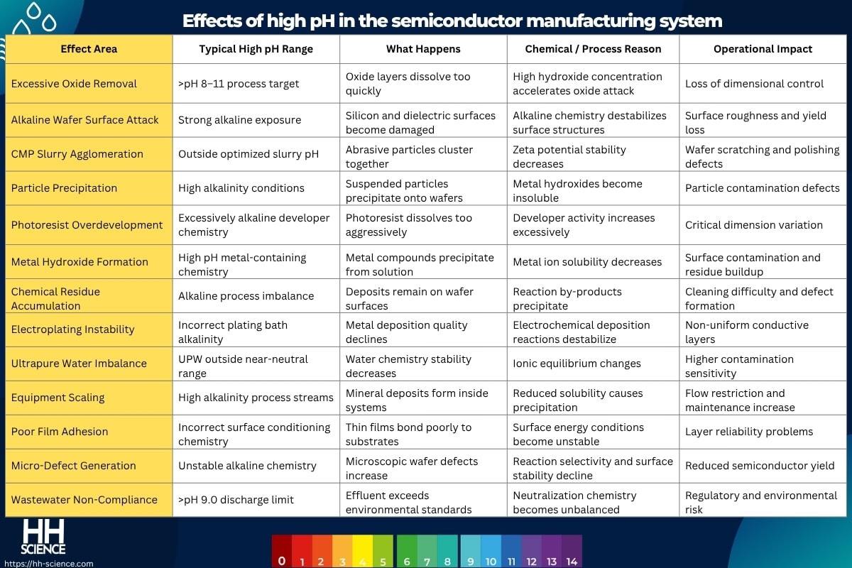
Effects of high pH in the semiconductor manufacturing system
High pH in semiconductor manufacturing systems can cause excessive oxide removal, alkaline wafer surface attack, CMP slurry agglomeration, particle precipitation, photoresist overdevelopment, metal hydroxide formation, chemical residue buildup, electroplating instability, ultrapure water imbalance, equipment scaling, poor film adhesion, micro-defect generation, and wastewater discharge non-compliance because excessive hydroxide ion (OH⁻) concentration changes chemical selectivity, destabilizes colloidal systems, reduces metal ion solubility, alters surface charge behavior, and accelerates alkaline reactions during sensitive semiconductor fabrication processes.
| Effect Area | Typical High pH Range | What Happens | Chemical / Process Reason | Operational Impact |
| Excessive Oxide Removal | >pH 8–11 process target | Oxide layers dissolve too quickly | High hydroxide concentration accelerates oxide attack | Loss of dimensional control |
| Alkaline Wafer Surface Attack | Strong alkaline exposure | Silicon and dielectric surfaces become damaged | Alkaline chemistry destabilizes surface structures | Surface roughness and yield loss |
| CMP Slurry Agglomeration | Outside optimized slurry pH | Abrasive particles cluster together | Zeta potential stability decreases | Wafer scratching and polishing defects |
| Particle Precipitation | High alkalinity conditions | Suspended particles precipitate onto wafers | Metal hydroxides become insoluble | Particle contamination defects |
| Photoresist Overdevelopment | Excessively alkaline developer chemistry | Photoresist dissolves too aggressively | Developer activity increases excessively | Critical dimension variation |
| Metal Hydroxide Formation | High pH metal-containing chemistry | Metal compounds precipitate from solution | Metal ion solubility decreases | Surface contamination and residue buildup |
| Chemical Residue Accumulation | Alkaline process imbalance | Deposits remain on wafer surfaces | Reaction by-products precipitate | Cleaning difficulty and defect formation |
| Electroplating Instability | Incorrect plating bath alkalinity | Metal deposition quality declines | Electrochemical deposition reactions destabilize | Non-uniform conductive layers |
| Ultrapure Water Imbalance | UPW outside near-neutral range | Water chemistry stability decreases | Ionic equilibrium changes | Higher contamination sensitivity |
| Equipment Scaling | High alkalinity process streams | Mineral deposits form inside systems | Reduced solubility causes precipitation | Flow restriction and maintenance increase |
| Poor Film Adhesion | Incorrect surface conditioning chemistry | Thin films bond poorly to substrates | Surface energy conditions become unstable | Layer reliability problems |
| Micro-Defect Generation | Unstable alkaline chemistry | Microscopic wafer defects increase | Reaction selectivity and surface stability decline | Reduced semiconductor yield |
| Wastewater Non-Compliance | >pH 9.0 discharge limit | Effluent exceeds environmental standards | Neutralization chemistry becomes unbalanced | Regulatory and environmental risk |
Operational, quality, and compliance risks
Operational, quality, and compliance risks in semiconductor manufacturing systems increase significantly when pH moves outside tightly controlled process windows because semiconductor fabrication depends on highly stable chemical reactions, ultra-low contamination conditions, precise surface chemistry, and nanometer-scale dimensional control throughout wafer cleaning, wet etching, CMP, lithography, electroplating, ultrapure water (UPW) treatment, and wastewater neutralization processes. Even small deviations from target ranges—such as approximately pH 2–5 for acidic etching baths, pH 8–11 for alkaline cleaning systems, controlled CMP slurry chemistry, near-neutral ultrapure water conditions with resistivity near 18.2 MΩ·cm, and pH 6.0–9.0 for wastewater discharge—can destabilize reaction kinetics, particle behavior, chemical selectivity, and contamination control, directly affecting semiconductor yield, equipment reliability, environmental compliance, and production cost.
- Wafer yield loss risk: Incorrect pH causes over-etching, under-etching, surface damage, particle contamination, and micro-defect formation that reduce usable wafer output and semiconductor device reliability.
- Critical dimension (CD) control risk: pH deviations in lithography and etching chemistries alter reaction rates and resist behavior, causing inaccurate nanoscale feature dimensions.
- CMP process instability risk: Improper slurry pH destabilizes abrasive dispersion, polishing rate, and zeta potential balance, increasing wafer scratching, dishing, erosion, and planarization defects.
- Particle contamination risk: Unstable pH changes colloidal stability and surface charge behavior, increasing particle agglomeration and adhesion on wafer surfaces.
- Metal contamination risk: Acidic conditions increase dissolved metal ion solubility, while alkaline conditions can precipitate metal hydroxides, both contributing to electrical defects and contamination failures.
- Ultrapure water (UPW) quality risk: UPW systems operating near 18.2 MΩ·cm resistivity are highly sensitive to pH imbalance, which can destabilize ionic equilibrium and reduce wafer cleanliness.
- Electroplating quality risk: Incorrect plating bath pH causes uneven metal deposition, void formation, conductivity variation, and poor interconnect reliability in semiconductor devices.
- Chemical selectivity loss: Out-of-range pH changes reaction preference between different wafer materials, reducing process precision and damaging adjacent structures.
- Equipment corrosion and scaling risk: Strong acidic or alkaline chemistries accelerate corrosion of stainless steel, quartz, and chemical delivery systems or promote scaling and residue buildup in fluid handling equipment.
- Film adhesion and surface integrity risk: Incorrect pH alters wafer surface chemistry and surface energy, causing thin-film adhesion failures, delamination, and reliability problems.
- Process repeatability risk: Small chemistry variations reduce batch-to-batch consistency and increase process drift across semiconductor production lines.
- Wastewater compliance risk: Semiconductor wastewater streams outside discharge limits such as pH 6.0–9.0 may violate environmental regulations and require additional neutralization treatment.
- Operational downtime and maintenance risk: pH instability increases cleaning frequency, tool maintenance, chemical replacement, sensor recalibration, and unscheduled process interruptions, raising manufacturing cost and reducing fab productivity.
pH measurement challenges in the semiconductor manufacturing system
pH measurement challenges in semiconductor manufacturing systems are driven by ultra-low ionic contamination requirements, high-purity chemical processing, nanometer-scale fabrication tolerances, aggressive acidic and alkaline chemistries, ultrapure water (UPW) systems with resistivity near 18.2 MΩ·cm, slurry particle interactions, temperature-sensitive reactions, dissolved metal contamination, and continuous inline monitoring demands across wet etching, CMP, electroplating, cleaning, lithography, and wastewater treatment processes. These conditions can affect electrode stability, reference junction performance, response time, contamination resistance, low-conductivity measurement accuracy, chemical compatibility, temperature compensation reliability, and long-term sensor drift, making specialized semiconductor-grade pH measurement technologies essential for stable process control, defect reduction, and high-yield semiconductor production.
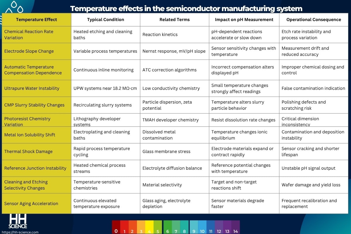
Temperature effects
Temperature effects are a major pH measurement challenge in semiconductor manufacturing systems because semiconductor fabrication processes involve highly temperature-sensitive chemical reactions where even small thermal variations can change hydrogen ion activity, chemical equilibrium, etch rate, slurry stability, photoresist behavior, metal ion solubility, and ultrapure water conductivity during wet etching, CMP, wafer cleaning, electroplating, and chemical delivery operations. Since many semiconductor processes require tight chemistry tolerances and stable pH control across conditions ranging from room-temperature ultrapure water systems to heated chemical baths and recirculating CMP slurries, improper temperature compensation, thermal drift, delayed equilibrium, or unstable process heating can cause inaccurate pH readings, process variation, wafer defects, contamination instability, and semiconductor yield loss.
| Temperature Effect | Typical Condition | Related Terms | Impact on pH Measurement | Operational Consequence |
| Chemical Reaction Rate Variation | Heated etching and cleaning baths | Reaction kinetics | pH-dependent reactions accelerate or slow down | Etch rate instability and process variation |
| Electrode Slope Change | Variable process temperatures | Nernst response, mV/pH slope | Sensor sensitivity changes with temperature | Measurement drift and reduced accuracy |
| Automatic Temperature Compensation Dependence | Continuous inline monitoring | ATC correction algorithms | Incorrect compensation alters displayed pH | Improper chemical dosing and control |
| Ultrapure Water Instability | UPW systems near 18.2 MΩ·cm | Low conductivity chemistry | Small temperature changes strongly affect readings | False contamination indication |
| CMP Slurry Stability Changes | Recirculating slurry systems | Particle dispersion, zeta potential | Temperature alters slurry particle behavior | Polishing defects and scratching risk |
| Photoresist Chemistry Variation | Lithography developer systems | TMAH developer chemistry | Resist dissolution rate changes | Critical dimension inconsistency |
| Metal Ion Solubility Shift | Electroplating and cleaning baths | Dissolved metal contamination | Temperature changes ionic equilibrium | Contamination and deposition instability |
| Thermal Shock Damage | Rapid process temperature cycling | Glass membrane stress | Electrode materials expand or contract rapidly | Sensor cracking and shorter lifespan |
| Reference Junction Instability | Heated chemical process streams | Electrolyte diffusion balance | Reference potential changes with temperature | Unstable pH signal output |
| Cleaning and Etching Selectivity Changes | Temperature-sensitive chemistries | Material selectivity | Target and non-target reactions shift | Wafer damage and yield loss |
| Sensor Aging Acceleration | Continuous elevated temperature exposure | Glass aging, electrolyte depletion | Sensor materials degrade faster | Frequent recalibration and replacement |
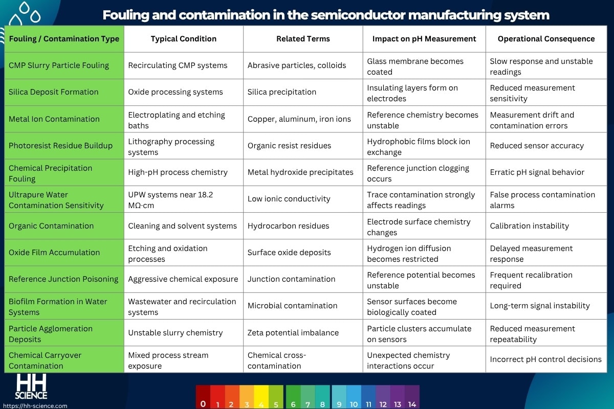
Fouling and contamination
Fouling and contamination are major pH measurement challenges in semiconductor manufacturing systems because semiconductor fabrication processes require extremely low contamination levels while continuously exposing sensors to CMP slurry particles, silica residues, metal ions, photoresist chemicals, oxide deposits, organic contaminants, chemical precipitates, and ultrapure water systems with very low ionic strength. These contaminants can coat the pH glass membrane, clog or poison the reference junction, alter hydrogen ion diffusion, destabilize low-conductivity measurements, increase electrical resistance, and cause slower response times, signal drift, unstable calibration, false contamination readings, and reduced sensor lifespan, directly affecting wafer cleanliness, process consistency, and semiconductor yield.
| Fouling / Contamination Type | Typical Condition | Related Terms | Impact on pH Measurement | Operational Consequence |
| CMP Slurry Particle Fouling | Recirculating CMP systems | Abrasive particles, colloids | Glass membrane becomes coated | Slow response and unstable readings |
| Silica Deposit Formation | Oxide processing systems | Silica precipitation | Insulating layers form on electrodes | Reduced measurement sensitivity |
| Metal Ion Contamination | Electroplating and etching baths | Copper, aluminum, iron ions | Reference chemistry becomes unstable | Measurement drift and contamination errors |
| Photoresist Residue Buildup | Lithography processing systems | Organic resist residues | Hydrophobic films block ion exchange | Reduced sensor accuracy |
| Chemical Precipitation Fouling | High-pH process chemistry | Metal hydroxide precipitates | Reference junction clogging occurs | Erratic pH signal behavior |
| Ultrapure Water Contamination Sensitivity | UPW systems near 18.2 MΩ·cm | Low ionic conductivity | Trace contamination strongly affects readings | False process contamination alarms |
| Organic Contamination | Cleaning and solvent systems | Hydrocarbon residues | Electrode surface chemistry changes | Calibration instability |
| Oxide Film Accumulation | Etching and oxidation processes | Surface oxide deposits | Hydrogen ion diffusion becomes restricted | Delayed measurement response |
| Reference Junction Poisoning | Aggressive chemical exposure | Junction contamination | Reference potential becomes unstable | Frequent recalibration required |
| Biofilm Formation in Water Systems | Wastewater and recirculation systems | Microbial contamination | Sensor surfaces become biologically coated | Long-term signal instability |
| Particle Agglomeration Deposits | Unstable slurry chemistry | Zeta potential imbalance | Particle clusters accumulate on sensors | Reduced measurement repeatability |
| Chemical Carryover Contamination | Mixed process stream exposure | Chemical cross-contamination | Unexpected chemistry interactions occur | Incorrect pH control decisions |
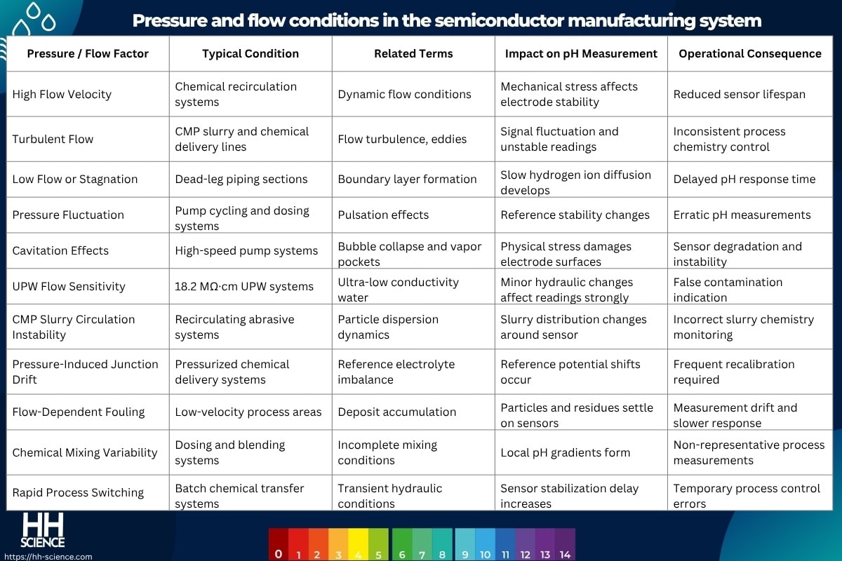
Pressure and flow conditions
Pressure and flow conditions are important pH measurement challenges in semiconductor manufacturing systems because wet processing tools, chemical delivery systems, CMP slurry circulation loops, ultrapure water (UPW) distribution networks, electroplating lines, filtration systems, and wastewater treatment processes all operate under controlled hydraulic conditions where pressure stability and flow behavior directly influence chemical uniformity, sensor response, and contamination control. Variations in flow velocity, turbulence, pressure fluctuation, stagnant zones, cavitation, or pulsating chemical delivery can disturb hydrogen ion diffusion at the electrode surface, destabilize low-conductivity measurements, introduce signal noise, accelerate fouling, and create non-representative chemistry readings that affect process precision, wafer quality, and semiconductor yield.
| Pressure / Flow Factor | Typical Condition | Related Terms | Impact on pH Measurement | Operational Consequence |
| High Flow Velocity | Chemical recirculation systems | Dynamic flow conditions | Mechanical stress affects electrode stability | Reduced sensor lifespan |
| Turbulent Flow | CMP slurry and chemical delivery lines | Flow turbulence, eddies | Signal fluctuation and unstable readings | Inconsistent process chemistry control |
| Low Flow or Stagnation | Dead-leg piping sections | Boundary layer formation | Slow hydrogen ion diffusion develops | Delayed pH response time |
| Pressure Fluctuation | Pump cycling and dosing systems | Pulsation effects | Reference stability changes | Erratic pH measurements |
| Cavitation Effects | High-speed pump systems | Bubble collapse and vapor pockets | Physical stress damages electrode surfaces | Sensor degradation and instability |
| UPW Flow Sensitivity | 18.2 MΩ·cm UPW systems | Ultra-low conductivity water | Minor hydraulic changes affect readings strongly | False contamination indication |
| CMP Slurry Circulation Instability | Recirculating abrasive systems | Particle dispersion dynamics | Slurry distribution changes around sensor | Incorrect slurry chemistry monitoring |
| Pressure-Induced Junction Drift | Pressurized chemical delivery systems | Reference electrolyte imbalance | Reference potential shifts occur | Frequent recalibration required |
| Flow-Dependent Fouling | Low-velocity process areas | Deposit accumulation | Particles and residues settle on sensors | Measurement drift and slower response |
| Chemical Mixing Variability | Dosing and blending systems | Incomplete mixing conditions | Local pH gradients form | Non-representative process measurements |
| Rapid Process Switching | Batch chemical transfer systems | Transient hydraulic conditions | Sensor stabilization delay increases | Temporary process control errors |
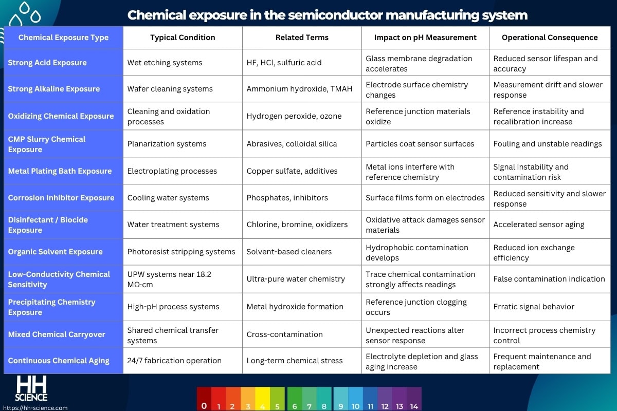
Chemical exposure (disinfectants, corrosion inhibitors)
Chemical exposure is a major pH measurement challenge in semiconductor manufacturing systems because sensors are continuously exposed to highly aggressive acidic and alkaline chemistries, oxidizers, solvents, CMP slurries, metal plating solutions, cleaning agents, corrosion inhibitors, biocides, and ultrapure water treatment chemicals used throughout wafer cleaning, wet etching, electroplating, lithography, cooling water treatment, and wastewater neutralization processes. These chemicals can attack glass membranes, poison or clog reference junctions, alter ionic activity, form insulating surface films, destabilize low-conductivity measurements, and accelerate sensor aging, leading to signal drift, unstable calibration, slower response, reduced measurement accuracy, and shortened operational lifespan in contamination-sensitive semiconductor fabrication environments.
| Chemical Exposure Type | Typical Condition | Related Terms | Impact on pH Measurement | Operational Consequence |
| Strong Acid Exposure | Wet etching systems | HF, HCl, sulfuric acid | Glass membrane degradation accelerates | Reduced sensor lifespan and accuracy |
| Strong Alkaline Exposure | Wafer cleaning systems | Ammonium hydroxide, TMAH | Electrode surface chemistry changes | Measurement drift and slower response |
| Oxidizing Chemical Exposure | Cleaning and oxidation processes | Hydrogen peroxide, ozone | Reference junction materials oxidize | Reference instability and recalibration increase |
| CMP Slurry Chemical Exposure | Planarization systems | Abrasives, colloidal silica | Particles coat sensor surfaces | Fouling and unstable readings |
| Metal Plating Bath Exposure | Electroplating processes | Copper sulfate, additives | Metal ions interfere with reference chemistry | Signal instability and contamination risk |
| Corrosion Inhibitor Exposure | Cooling water systems | Phosphates, inhibitors | Surface films form on electrodes | Reduced sensitivity and slower response |
| Disinfectant / Biocide Exposure | Water treatment systems | Chlorine, bromine, oxidizers | Oxidative attack damages sensor materials | Accelerated sensor aging |
| Organic Solvent Exposure | Photoresist stripping systems | Solvent-based cleaners | Hydrophobic contamination develops | Reduced ion exchange efficiency |
| Low-Conductivity Chemical Sensitivity | UPW systems near 18.2 MΩ·cm | Ultra-pure water chemistry | Trace chemical contamination strongly affects readings | False contamination indication |
| Precipitating Chemistry Exposure | High-pH process systems | Metal hydroxide formation | Reference junction clogging occurs | Erratic signal behavior |
| Mixed Chemical Carryover | Shared chemical transfer systems | Cross-contamination | Unexpected reactions alter sensor response | Incorrect process chemistry control |
| Continuous Chemical Aging | 24/7 fabrication operation | Long-term chemical stress | Electrolyte depletion and glass aging increase | Frequent maintenance and replacement |
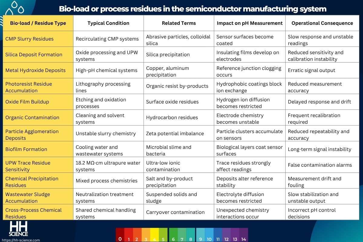
Bio-load or process residues
Bio-load and process residues are significant pH measurement challenges in semiconductor manufacturing systems because semiconductor fabrication environments continuously generate chemical residues, slurry particles, silica deposits, metal hydroxides, photoresist by-products, oxide films, organic contamination, and microbial growth in water treatment and wastewater systems that can accumulate on sensor surfaces and interfere with accurate measurement. These deposits affect hydrogen ion diffusion, clog reference junctions, alter surface conductivity, destabilize low-conductivity ultrapure water measurements near 18.2 MΩ·cm, increase electrical resistance, and cause slower response times, signal drift, unstable calibration, false contamination indications, and reduced sensor lifespan in contamination-sensitive semiconductor processes.
| Bio-load / Residue Type | Typical Condition | Related Terms | Impact on pH Measurement | Operational Consequence |
| CMP Slurry Residues | Recirculating CMP systems | Abrasive particles, colloidal silica | Sensor surfaces become coated | Slow response and unstable readings |
| Silica Deposit Formation | Oxide processing and UPW systems | Silica precipitation | Insulating films develop on electrodes | Reduced sensitivity and calibration instability |
| Metal Hydroxide Deposits | High-pH chemical systems | Copper, aluminum precipitation | Reference junction clogging occurs | Erratic signal output |
| Photoresist Residue Accumulation | Lithography processing lines | Organic resist by-products | Hydrophobic coatings block ion exchange | Reduced measurement accuracy |
| Oxide Film Buildup | Etching and oxidation processes | Surface oxide residues | Hydrogen ion diffusion becomes restricted | Delayed response and drift |
| Organic Contamination | Cleaning and solvent systems | Hydrocarbon residues | Electrode chemistry becomes unstable | Frequent recalibration required |
| Particle Agglomeration Deposits | Unstable slurry chemistry | Zeta potential imbalance | Particle clusters accumulate on sensors | Reduced repeatability and accuracy |
| Biofilm Formation | Cooling water and wastewater systems | Microbial slime and bacteria | Biological layers coat sensor surfaces | Long-term signal instability |
| UPW Trace Residue Sensitivity | 18.2 MΩ·cm ultrapure water systems | Ultra-low ionic contamination | Trace residues strongly affect readings | False contamination alarms |
| Chemical Precipitation Residues | Mixed process chemistries | Salt and by-product precipitation | Deposits alter reference stability | Measurement drift and fouling |
| Wastewater Sludge Accumulation | Neutralization treatment systems | Suspended solids and sludge | Electrolyte diffusion becomes restricted | Slow stabilization and unstable output |
| Cross-Process Chemical Residues | Shared chemical handling systems | Carryover contamination | Unexpected chemistry interactions occur | Incorrect pH control decisions |
Common pH sensor types used in semiconductor manufacturing systems
Common pH sensor types used in semiconductor manufacturing systems include low-conductivity combination pH sensors, differential pH sensors, double- and triple-junction reference electrodes, ISFET and solid-state pH sensors, high-purity inline pH probes, digital or smart pH sensors, flow-through sample chamber sensors, immersion sensors, retractable sanitary sensors, and chemically resistant semiconductor-grade electrodes designed for ultrapure water (UPW), CMP slurry, wet etching, electroplating, cleaning, and wastewater treatment applications. These sensor technologies are selected to maintain highly stable and contamination-resistant measurement in ultra-low ionic conductivity systems near 18.2 MΩ·cm, aggressive acidic and alkaline chemistries such as pH 2–5 etching baths and pH 8–11 cleaning solutions, particle-loaded CMP slurries, and high-purity chemical delivery systems while minimizing metal contamination, reference poisoning, fouling, signal drift, and process instability in nanometer-scale semiconductor fabrication environments.
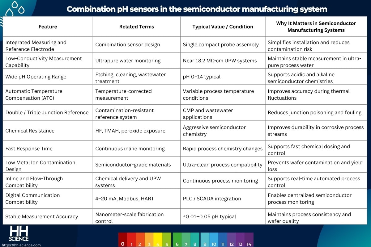
Combination pH sensors
Combination pH sensors are widely used in semiconductor manufacturing systems because they integrate the measuring electrode and reference electrode into a single compact assembly, allowing stable, contamination-controlled, and high-accuracy monitoring in ultrapure water (UPW) systems, wet etching baths, wafer cleaning systems, CMP slurry loops, electroplating lines, chemical delivery systems, and wastewater neutralization processes. Their compact design, low ionic contamination compatibility, chemical resistance, automatic temperature compensation (ATC), and ability to maintain stable measurement in aggressive acidic and alkaline chemistries make them highly suitable for semiconductor fabrication environments requiring tight process control, low defect generation, and continuous inline monitoring.
| Feature | Related Terms | Typical Value / Condition | Why It Matters in Semiconductor Manufacturing Systems |
| Integrated Measuring and Reference Electrode | Combination sensor design | Single compact probe assembly | Simplifies installation and reduces contamination risk |
| Low-Conductivity Measurement Capability | Ultrapure water monitoring | Near 18.2 MΩ·cm UPW systems | Maintains stable measurement in ultra-pure process water |
| Wide pH Operating Range | Etching, cleaning, wastewater treatment | pH 0–14 typical | Supports acidic and alkaline semiconductor chemistries |
| Automatic Temperature Compensation (ATC) | Temperature-corrected measurement | Variable process temperature conditions | Improves accuracy during thermal fluctuations |
| Double / Triple Junction Reference | Contamination-resistant reference system | CMP and wastewater applications | Reduces junction poisoning and fouling |
| Chemical Resistance | HF, TMAH, peroxide exposure | Aggressive semiconductor chemistry | Improves durability in corrosive process streams |
| Fast Response Time | Continuous inline monitoring | Rapid process chemistry changes | Supports fast chemical dosing and control |
| Low Metal Ion Contamination Design | Semiconductor-grade materials | Ultra-clean process compatibility | Prevents wafer contamination and yield loss |
| Inline and Flow-Through Compatibility | Chemical delivery and UPW systems | Continuous process monitoring | Supports real-time automated process control |
| Digital Communication Compatibility | 4–20 mA, Modbus, HART | PLC / SCADA integration | Enables centralized semiconductor process monitoring |
| Stable Measurement Accuracy | Nanometer-scale fabrication control | ±0.01–0.05 pH typical | Maintains process consistency and wafer quality |
Differential pH sensors
Differential pH sensors are highly suitable for semiconductor manufacturing systems because they provide stable and contamination-resistant measurement in applications where conventional reference junctions are vulnerable to fouling, slurry particles, metal contamination, silica deposits, photoresist residues, aggressive chemistries, and ultra-low conductivity ultrapure water (UPW) conditions. By using a differential measurement architecture with multiple glass electrodes and an internally buffered reference system instead of a traditional liquid junction, these sensors reduce reference poisoning, improve long-term stability, minimize drift in high-purity process streams, and maintain reliable accuracy in CMP slurry systems, wet etching baths, chemical delivery loops, wastewater treatment systems, and semiconductor-grade UPW applications.
| Feature | Related Terms | Typical Value / Condition | Why It Matters in Semiconductor Manufacturing Systems |
| Differential Measurement Architecture | Dual glass electrode design | No conventional liquid junction | Improves stability in contaminated and low-conductivity environments |
| Buffered Internal Reference System | Stable internal electrolyte | Isolated reference chamber | Reduces reference drift and poisoning |
| Low-Conductivity Water Compatibility | Ultrapure water systems | Near 18.2 MΩ·cm resistivity | Maintains stable measurement in UPW applications |
| High Fouling Resistance | CMP slurry and wastewater systems | Silica, particles, sludge exposure | Minimizes instability caused by deposits and residues |
| Chemical Resistance | HF, TMAH, peroxide exposure | Aggressive semiconductor chemistry | Improves durability in corrosive process streams |
| Reduced Metal Contamination Risk | Semiconductor-grade materials | Ultra-clean process compatibility | Protects wafer surfaces from contamination defects |
| Stable Signal Output | Continuous inline process monitoring | Low-noise measurement | Supports reliable automated chemistry control |
| Automatic Temperature Compensation (ATC) | Temperature-corrected measurement | Variable process temperature conditions | Maintains accuracy during thermal fluctuations |
| Extended Maintenance Interval | Low-maintenance sensor design | Reduced recalibration frequency | Improves process uptime and maintenance efficiency |
| Inline and Flow-Through Compatibility | Chemical delivery and UPW systems | Continuous process monitoring | Supports real-time semiconductor process control |
| Stable Measurement Accuracy | Nanometer-scale fabrication control | ±0.01–0.05 pH typical | Maintains wafer quality and process repeatability |

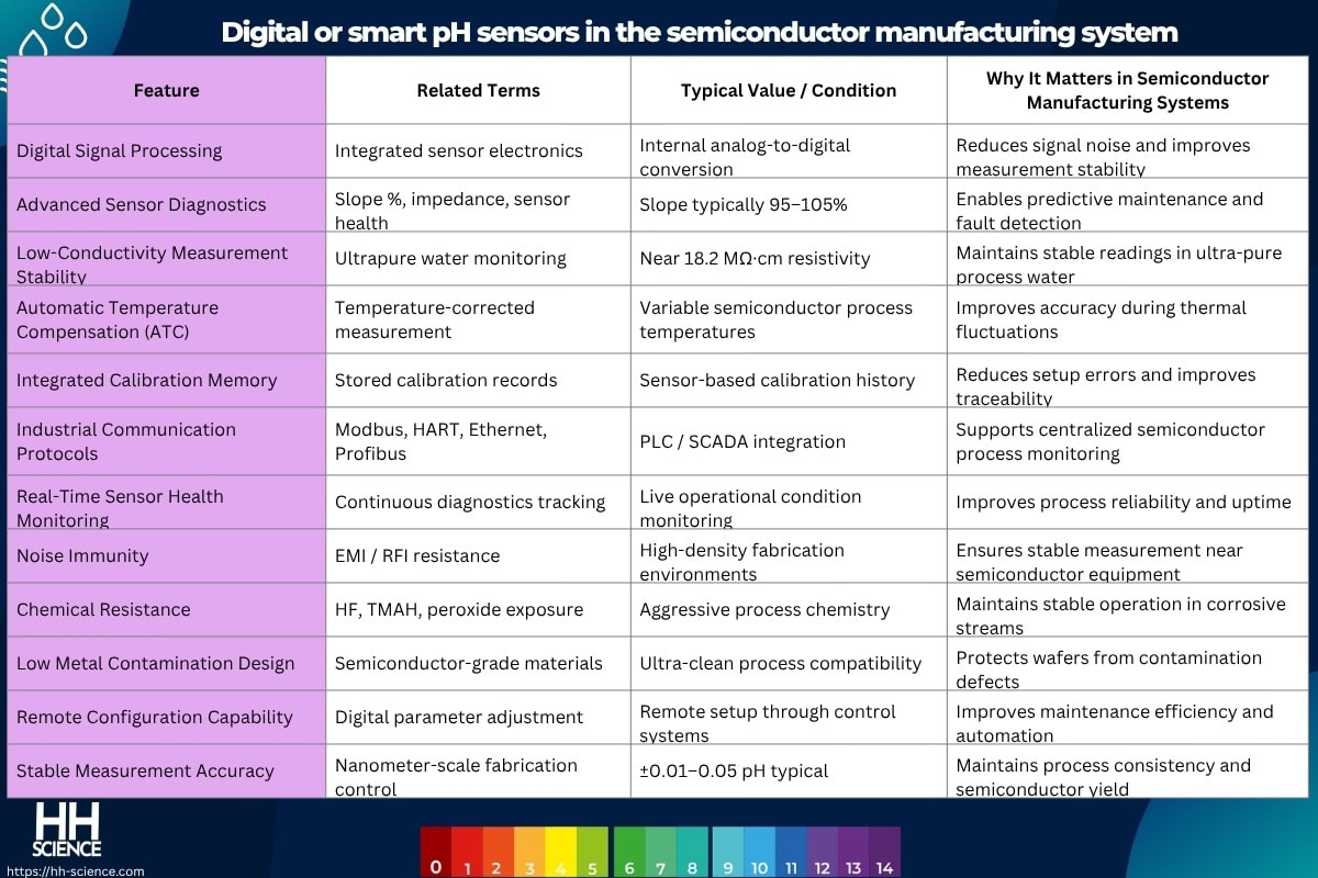
Digital or smart pH sensors
Digital or smart pH sensors are highly suitable for semiconductor manufacturing systems because they provide stable, low-noise, contamination-resistant, and diagnostics-driven measurement in ultrapure water (UPW) systems, CMP slurry loops, wet etching baths, electroplating lines, wafer cleaning systems, chemical delivery networks, and wastewater treatment processes where nanometer-scale fabrication tolerances require highly accurate and continuous chemistry control. By converting analog signals into digital data directly inside the sensor, they minimize electrical interference, improve low-conductivity measurement stability near 18.2 MΩ·cm, support predictive diagnostics, reduce calibration errors, and maintain highly reliable accuracy (typically ±0.01–0.05 pH) in chemically aggressive and contamination-sensitive semiconductor production environments.
| Feature | Related Terms | Typical Value / Condition | Why It Matters in Semiconductor Manufacturing Systems |
| Digital Signal Processing | Integrated sensor electronics | Internal analog-to-digital conversion | Reduces signal noise and improves measurement stability |
| Advanced Sensor Diagnostics | Slope %, impedance, sensor health | Slope typically 95–105% | Enables predictive maintenance and fault detection |
| Low-Conductivity Measurement Stability | Ultrapure water monitoring | Near 18.2 MΩ·cm resistivity | Maintains stable readings in ultra-pure process water |
| Automatic Temperature Compensation (ATC) | Temperature-corrected measurement | Variable semiconductor process temperatures | Improves accuracy during thermal fluctuations |
| Integrated Calibration Memory | Stored calibration records | Sensor-based calibration history | Reduces setup errors and improves traceability |
| Industrial Communication Protocols | Modbus, HART, Ethernet, Profibus | PLC / SCADA integration | Supports centralized semiconductor process monitoring |
| Real-Time Sensor Health Monitoring | Continuous diagnostics tracking | Live operational condition monitoring | Improves process reliability and uptime |
| Noise Immunity | EMI / RFI resistance | High-density fabrication environments | Ensures stable measurement near semiconductor equipment |
| Chemical Resistance | HF, TMAH, peroxide exposure | Aggressive process chemistry | Maintains stable operation in corrosive streams |
| Low Metal Contamination Design | Semiconductor-grade materials | Ultra-clean process compatibility | Protects wafers from contamination defects |
| Remote Configuration Capability | Digital parameter adjustment | Remote setup through control systems | Improves maintenance efficiency and automation |
| Stable Measurement Accuracy | Nanometer-scale fabrication control | ±0.01–0.05 pH typical | Maintains process consistency and semiconductor yield |
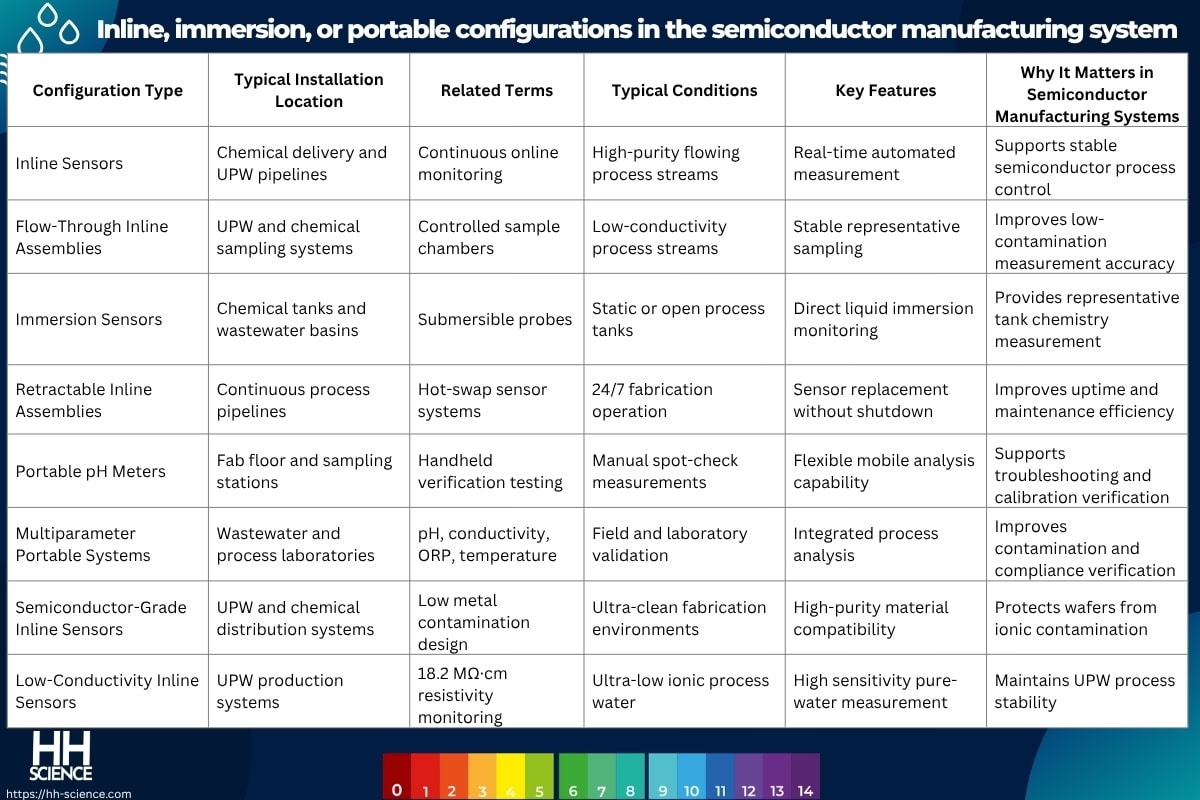
Inline, immersion, or portable configurations
Inline, immersion, and portable pH sensor configurations are all used in semiconductor manufacturing systems because different fabrication processes—such as ultrapure water (UPW) production, wet etching, CMP slurry circulation, wafer cleaning, electroplating, chemical delivery, and wastewater neutralization—require different installation approaches depending on contamination sensitivity, flow conditions, chemical aggressiveness, maintenance accessibility, and process control requirements. Inline configurations support continuous real-time monitoring in automated production lines, immersion sensors are used in chemical tanks and treatment basins, and portable pH systems provide field verification, calibration confirmation, troubleshooting, and independent chemistry validation while maintaining tightly controlled process conditions such as pH 2–5 for etching baths, pH 8–11 for cleaning systems, and near-neutral conditions in UPW systems with resistivity near 18.2 MΩ·cm.
| Configuration Type | Typical Installation Location | Related Terms | Typical Conditions | Key Features | Why It Matters in Semiconductor Manufacturing Systems |
| Inline Sensors | Chemical delivery and UPW pipelines | Continuous online monitoring | High-purity flowing process streams | Real-time automated measurement | Supports stable semiconductor process control |
| Flow-Through Inline Assemblies | UPW and chemical sampling systems | Controlled sample chambers | Low-conductivity process streams | Stable representative sampling | Improves low-contamination measurement accuracy |
| Immersion Sensors | Chemical tanks and wastewater basins | Submersible probes | Static or open process tanks | Direct liquid immersion monitoring | Provides representative tank chemistry measurement |
| Retractable Inline Assemblies | Continuous process pipelines | Hot-swap sensor systems | 24/7 fabrication operation | Sensor replacement without shutdown | Improves uptime and maintenance efficiency |
| Portable pH Meters | Fab floor and sampling stations | Handheld verification testing | Manual spot-check measurements | Flexible mobile analysis capability | Supports troubleshooting and calibration verification |
| Multiparameter Portable Systems | Wastewater and process laboratories | pH, conductivity, ORP, temperature | Field and laboratory validation | Integrated process analysis | Improves contamination and compliance verification |
| Semiconductor-Grade Inline Sensors | UPW and chemical distribution systems | Low metal contamination design | Ultra-clean fabrication environments | High-purity material compatibility | Protects wafers from ionic contamination |
| Low-Conductivity Inline Sensors | UPW production systems | 18.2 MΩ·cm resistivity monitoring | Ultra-low ionic process water | High sensitivity pure-water measurement | Maintains UPW process stability |
Installation and maintenance considerations in a semiconductor manufacturing system
Installation and maintenance considerations in semiconductor manufacturing systems are critical because pH sensors must operate reliably in ultra-clean and contamination-sensitive environments involving ultrapure water (UPW) systems with resistivity near 18.2 MΩ·cm, aggressive acidic and alkaline chemistries such as pH 2–5 etching baths and pH 8–11 cleaning solutions, CMP slurry circulation loops, electroplating systems, chemical delivery lines, and wastewater neutralization processes where even trace contamination or unstable measurement can affect wafer yield and process precision. Proper installation in representative flow locations with controlled pressure, stable temperature, low dead-volume sampling, contamination-resistant wetted materials, and optimized hydraulic conditions—combined with regular calibration using traceable buffers (pH 4.01, 7.00, 10.01), cleaning to remove slurry particles, silica deposits, metal hydroxides, photoresist residues, and chemical precipitates, and monitoring of reference junction condition, electrode slope (typically 95–105%), response time, and automatic temperature compensation (ATC)—is essential to maintain highly accurate measurement (typically ±0.01–0.05 pH), stable semiconductor chemistry control, low defect density, and long-term fabrication reliability.
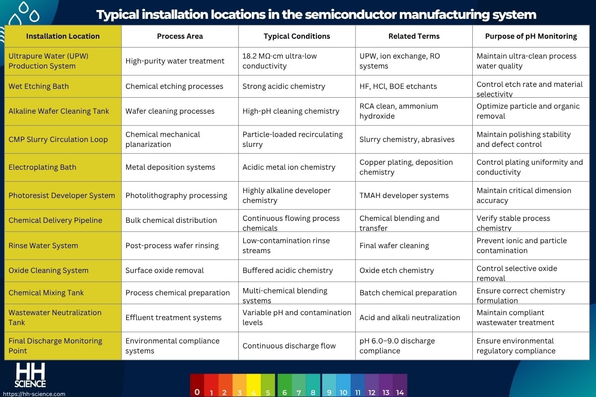
Typical installation locations
Typical pH sensor installation locations in semiconductor manufacturing systems are selected at critical process control points where wafer surface chemistry, contamination control, chemical stability, ultrapure water quality, slurry performance, and wastewater compliance depend on highly stable and accurate pH monitoring. These locations include ultrapure water (UPW) production systems, wet etching baths, wafer cleaning stations, CMP slurry circulation loops, electroplating tanks, chemical delivery systems, photoresist developer lines, rinse water systems, and wastewater neutralization units, each requiring specific installation methods based on contamination sensitivity, chemical aggressiveness, flow stability, and process automation requirements.
| Installation Location | Process Area | Typical Conditions | Related Terms | Purpose of pH Monitoring |
| Ultrapure Water (UPW) Production System | High-purity water treatment | 18.2 MΩ·cm ultra-low conductivity | UPW, ion exchange, RO systems | Maintain ultra-clean process water quality |
| Wet Etching Bath | Chemical etching processes | Strong acidic chemistry | HF, HCl, BOE etchants | Control etch rate and material selectivity |
| Alkaline Wafer Cleaning Tank | Wafer cleaning processes | High-pH cleaning chemistry | RCA clean, ammonium hydroxide | Optimize particle and organic removal |
| CMP Slurry Circulation Loop | Chemical mechanical planarization | Particle-loaded recirculating slurry | Slurry chemistry, abrasives | Maintain polishing stability and defect control |
| Electroplating Bath | Metal deposition systems | Acidic metal ion chemistry | Copper plating, deposition chemistry | Control plating uniformity and conductivity |
| Photoresist Developer System | Photolithography processing | Highly alkaline developer chemistry | TMAH developer systems | Maintain critical dimension accuracy |
| Chemical Delivery Pipeline | Bulk chemical distribution | Continuous flowing process chemicals | Chemical blending and transfer | Verify stable process chemistry |
| Rinse Water System | Post-process wafer rinsing | Low-contamination rinse streams | Final wafer cleaning | Prevent ionic and particle contamination |
| Oxide Cleaning System | Surface oxide removal | Buffered acidic chemistry | Oxide etch chemistry | Control selective oxide removal |
| Chemical Mixing Tank | Process chemical preparation | Multi-chemical blending systems | Batch chemical preparation | Ensure correct chemistry formulation |
| Wastewater Neutralization Tank | Effluent treatment systems | Variable pH and contamination levels | Acid and alkali neutralization | Maintain compliant wastewater treatment |
| Final Discharge Monitoring Point | Environmental compliance systems | Continuous discharge flow | pH 6.0–9.0 discharge compliance | Ensure environmental regulatory compliance |
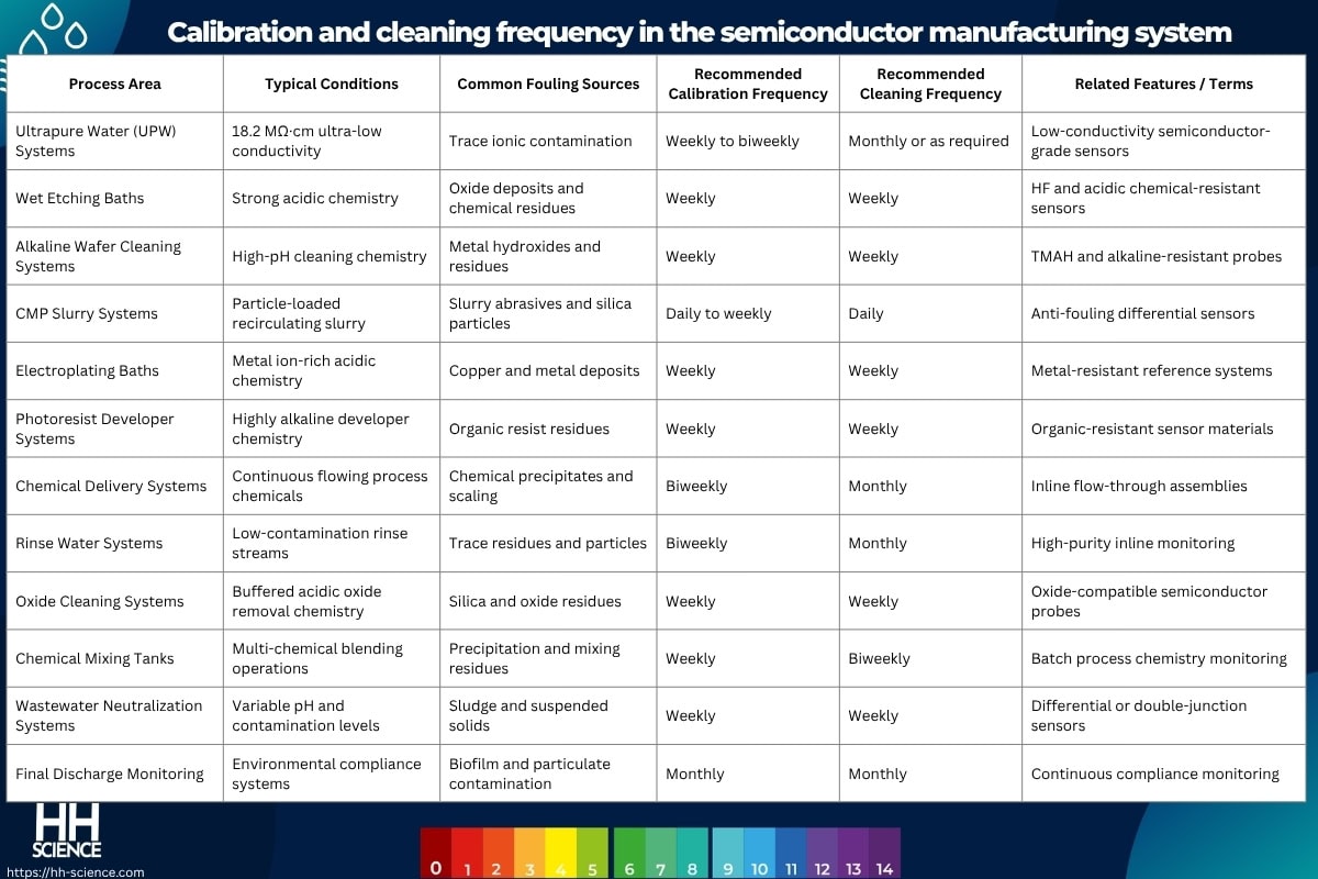
Calibration and cleaning frequency
Calibration and cleaning frequency in semiconductor manufacturing systems depend on factors such as ultrapure water (UPW) purity near 18.2 MΩ·cm, aggressive acidic and alkaline chemistries, CMP slurry particle loading, metal ion contamination, photoresist residues, silica deposits, continuous inline operation, and contamination sensitivity across wet etching, wafer cleaning, electroplating, chemical delivery, and wastewater treatment processes. To maintain highly accurate measurement (typically ±0.01–0.05 pH) and stable semiconductor process control, sensors are routinely calibrated using traceable semiconductor-grade buffers (pH 4.01, 7.00, 10.01) and cleaned to remove slurry particles, silica scale, organic residues, metal hydroxides, and chemical precipitates that can destabilize low-conductivity measurements and affect wafer yield.
| Process Area | Typical Conditions | Common Fouling Sources | Recommended Calibration Frequency | Recommended Cleaning Frequency | Related Features / Terms |
| Ultrapure Water (UPW) Systems | 18.2 MΩ·cm ultra-low conductivity | Trace ionic contamination | Weekly to biweekly | Monthly or as required | Low-conductivity semiconductor-grade sensors |
| Wet Etching Baths | Strong acidic chemistry | Oxide deposits and chemical residues | Weekly | Weekly | HF and acidic chemical-resistant sensors |
| Alkaline Wafer Cleaning Systems | High-pH cleaning chemistry | Metal hydroxides and residues | Weekly | Weekly | TMAH and alkaline-resistant probes |
| CMP Slurry Systems | Particle-loaded recirculating slurry | Slurry abrasives and silica particles | Daily to weekly | Daily | Anti-fouling differential sensors |
| Electroplating Baths | Metal ion-rich acidic chemistry | Copper and metal deposits | Weekly | Weekly | Metal-resistant reference systems |
| Photoresist Developer Systems | Highly alkaline developer chemistry | Organic resist residues | Weekly | Weekly | Organic-resistant sensor materials |
| Chemical Delivery Systems | Continuous flowing process chemicals | Chemical precipitates and scaling | Biweekly | Monthly | Inline flow-through assemblies |
| Rinse Water Systems | Low-contamination rinse streams | Trace residues and particles | Biweekly | Monthly | High-purity inline monitoring |
| Oxide Cleaning Systems | Buffered acidic oxide removal chemistry | Silica and oxide residues | Weekly | Weekly | Oxide-compatible semiconductor probes |
| Chemical Mixing Tanks | Multi-chemical blending operations | Precipitation and mixing residues | Weekly | Biweekly | Batch process chemistry monitoring |
| Wastewater Neutralization Systems | Variable pH and contamination levels | Sludge and suspended solids | Weekly | Weekly | Differential or double-junction sensors |
| Final Discharge Monitoring | Environmental compliance systems | Biofilm and particulate contamination | Monthly | Monthly | Continuous compliance monitoring |
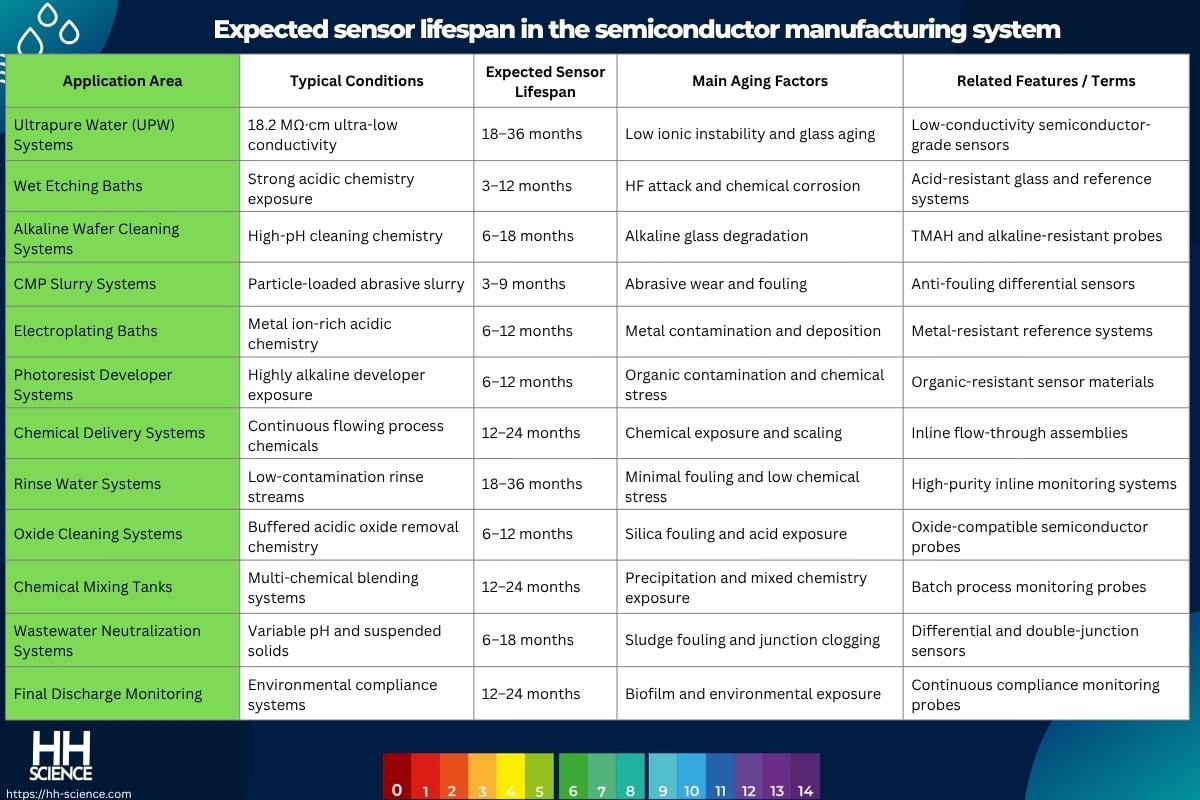
Expected sensor lifespan
Expected pH sensor lifespan in semiconductor manufacturing systems varies depending on ultrapure water purity, exposure to aggressive acidic and alkaline chemistries, CMP slurry particle loading, metal ion contamination, temperature cycling, organic solvent exposure, cleaning frequency, and continuous inline operation across wet etching, wafer cleaning, electroplating, chemical delivery, and wastewater treatment processes. Sensors operating in clean low-conductivity UPW systems may last several years, while probes exposed to abrasive CMP slurries, hydrofluoric acid (HF), strong alkaline developers, metal plating baths, or heavy fouling conditions typically experience accelerated glass aging, reference degradation, junction poisoning, and faster calibration drift.
| Application Area | Typical Conditions | Expected Sensor Lifespan | Main Aging Factors | Related Features / Terms |
| Ultrapure Water (UPW) Systems | 18.2 MΩ·cm ultra-low conductivity | 18–36 months | Low ionic instability and glass aging | Low-conductivity semiconductor-grade sensors |
| Wet Etching Baths | Strong acidic chemistry exposure | 3–12 months | HF attack and chemical corrosion | Acid-resistant glass and reference systems |
| Alkaline Wafer Cleaning Systems | High-pH cleaning chemistry | 6–18 months | Alkaline glass degradation | TMAH and alkaline-resistant probes |
| CMP Slurry Systems | Particle-loaded abrasive slurry | 3–9 months | Abrasive wear and fouling | Anti-fouling differential sensors |
| Electroplating Baths | Metal ion-rich acidic chemistry | 6–12 months | Metal contamination and deposition | Metal-resistant reference systems |
| Photoresist Developer Systems | Highly alkaline developer exposure | 6–12 months | Organic contamination and chemical stress | Organic-resistant sensor materials |
| Chemical Delivery Systems | Continuous flowing process chemicals | 12–24 months | Chemical exposure and scaling | Inline flow-through assemblies |
| Rinse Water Systems | Low-contamination rinse streams | 18–36 months | Minimal fouling and low chemical stress | High-purity inline monitoring systems |
| Oxide Cleaning Systems | Buffered acidic oxide removal chemistry | 6–12 months | Silica fouling and acid exposure | Oxide-compatible semiconductor probes |
| Chemical Mixing Tanks | Multi-chemical blending systems | 12–24 months | Precipitation and mixed chemistry exposure | Batch process monitoring probes |
| Wastewater Neutralization Systems | Variable pH and suspended solids | 6–18 months | Sludge fouling and junction clogging | Differential and double-junction sensors |
| Final Discharge Monitoring | Environmental compliance systems | 12–24 months | Biofilm and environmental exposure | Continuous compliance monitoring probes |
Trade-offs between accuracy, maintenance, and durability
In semiconductor manufacturing systems, trade-offs between accuracy, maintenance, and durability occur because pH sensors must maintain extremely stable measurement (typically ±0.01–0.05 pH) in ultrapure water (UPW) systems near 18.2 MΩ·cm, aggressive acidic and alkaline chemistries, abrasive CMP slurry loops, metal plating baths, and contamination-sensitive nanometer-scale fabrication processes where even very small measurement drift can affect wafer yield and process precision. High-accuracy semiconductor-grade sensors designed for ultra-low conductivity UPW monitoring and critical etching or lithography applications often use highly sensitive glass membranes, low-contamination reference systems, and precision temperature compensation that provide superior response stability and low ionic sensitivity but require more frequent calibration, stricter cleaning procedures, and shorter replacement intervals due to chemical attack, slurry abrasion, metal contamination, and reference poisoning, whereas more durable differential or double-junction sensors with reinforced reference systems, anti-fouling designs, and chemically resistant materials can better tolerate CMP particles, sludge, metal hydroxides, peroxide exposure, and continuous wastewater operation with lower maintenance frequency, but may respond more slowly or provide slightly lower sensitivity in ultra-pure semiconductor chemistry applications where maximum process accuracy is critical.
Regulatory or quality considerations in a semiconductor manufacturing system
Regulatory and quality considerations in semiconductor manufacturing systems are critical because pH directly affects wafer surface chemistry, wet etching precision, CMP slurry stability, ultrapure water (UPW) purity, metal contamination control, photoresist processing, electroplating performance, particle defect prevention, equipment corrosion resistance, and wastewater neutralization across highly sensitive nanometer-scale fabrication processes. Maintaining tightly controlled chemistry targets—such as approximately pH 2–5 for acidic etching systems, pH 8–11 for alkaline cleaning chemistries, near-neutral conditions in UPW systems with resistivity near 18.2 MΩ·cm, and pH 6.0–9.0 for wastewater discharge—through continuous inline monitoring, semiconductor-grade low-contamination sensors, traceable calibration buffers (pH 4.01, 7.00, 10.01), automatic temperature compensation (ATC), chemical-resistant materials, and integrated PLC/SCADA process control is essential to maintain semiconductor yield, reduce defect density, comply with environmental discharge regulations, support ISO quality systems, and ensure stable high-volume semiconductor production.
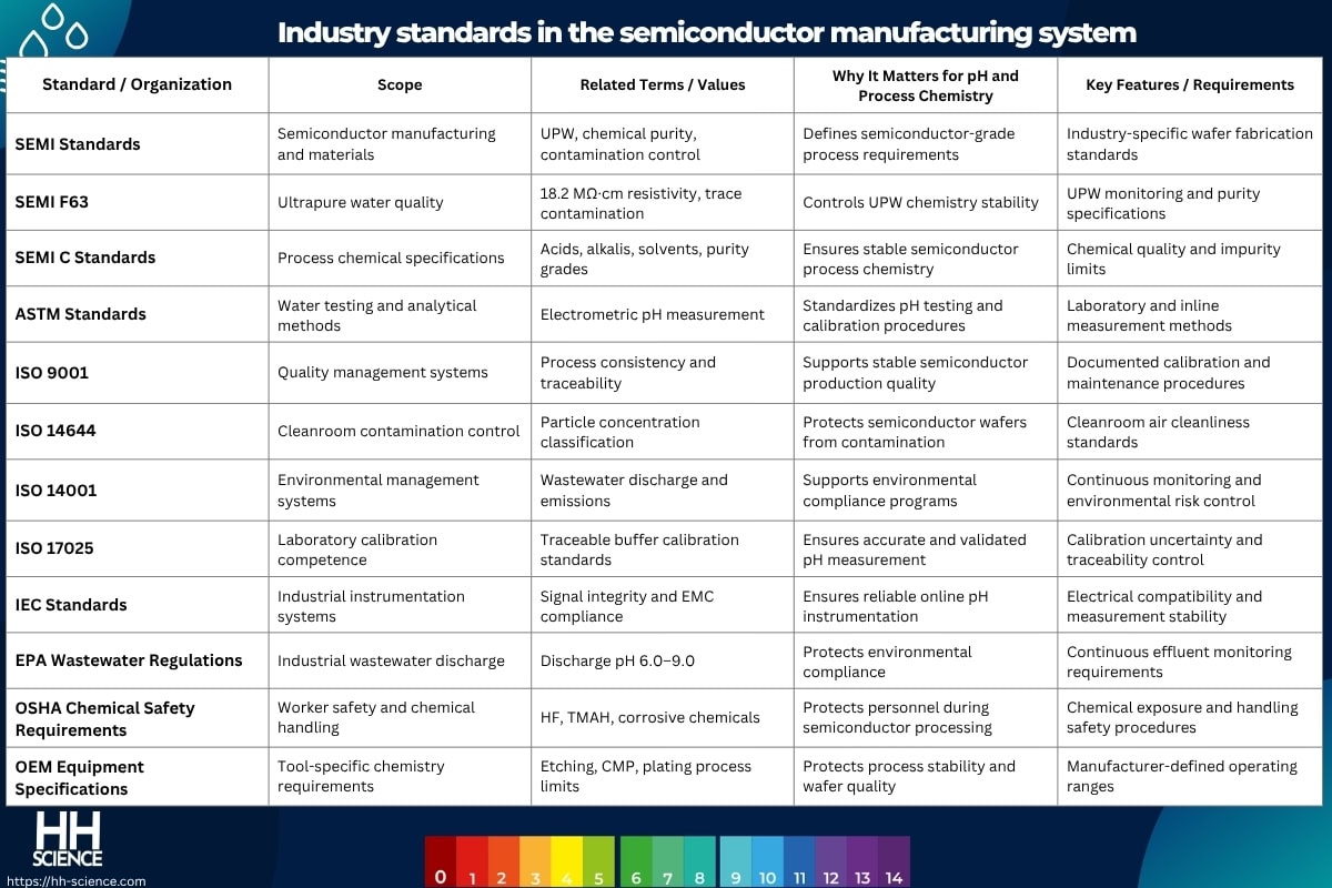
Industry standards in the semiconductor manufacturing system
Industry standards in semiconductor manufacturing systems define the required practices for ultrapure water (UPW) quality, chemical contamination control, semiconductor process consistency, wastewater discharge compliance, cleanroom operation, analytical measurement accuracy, and equipment reliability to ensure stable nanometer-scale wafer fabrication and high semiconductor yield. These standards establish limits and best practices for parameters such as pH, resistivity, conductivity, dissolved silica, total organic carbon (TOC), trace metals, particles, chemical purity, wastewater discharge chemistry, and calibration traceability, helping semiconductor fabs minimize contamination defects, corrosion, process instability, wafer damage, and environmental compliance risk.
| Standard / Organization | Scope | Related Terms / Values | Why It Matters for pH and Process Chemistry | Key Features / Requirements |
| SEMI Standards | Semiconductor manufacturing and materials | UPW, chemical purity, contamination control | Defines semiconductor-grade process requirements | Industry-specific wafer fabrication standards |
| SEMI F63 | Ultrapure water quality | 18.2 MΩ·cm resistivity, trace contamination | Controls UPW chemistry stability | UPW monitoring and purity specifications |
| SEMI C Standards | Process chemical specifications | Acids, alkalis, solvents, purity grades | Ensures stable semiconductor process chemistry | Chemical quality and impurity limits |
| ASTM Standards | Water testing and analytical methods | Electrometric pH measurement | Standardizes pH testing and calibration procedures | Laboratory and inline measurement methods |
| ISO 9001 | Quality management systems | Process consistency and traceability | Supports stable semiconductor production quality | Documented calibration and maintenance procedures |
| ISO 14644 | Cleanroom contamination control | Particle concentration classification | Protects semiconductor wafers from contamination | Cleanroom air cleanliness standards |
| ISO 14001 | Environmental management systems | Wastewater discharge and emissions | Supports environmental compliance programs | Continuous monitoring and environmental risk control |
| ISO 17025 | Laboratory calibration competence | Traceable buffer calibration standards | Ensures accurate and validated pH measurement | Calibration uncertainty and traceability control |
| IEC Standards | Industrial instrumentation systems | Signal integrity and EMC compliance | Ensures reliable online pH instrumentation | Electrical compatibility and measurement stability |
| EPA Wastewater Regulations | Industrial wastewater discharge | Discharge pH 6.0–9.0 | Protects environmental compliance | Continuous effluent monitoring requirements |
| OSHA Chemical Safety Requirements | Worker safety and chemical handling | HF, TMAH, corrosive chemicals | Protects personnel during semiconductor processing | Chemical exposure and handling safety procedures |
| OEM Equipment Specifications | Tool-specific chemistry requirements | Etching, CMP, plating process limits | Protects process stability and wafer quality | Manufacturer-defined operating ranges |
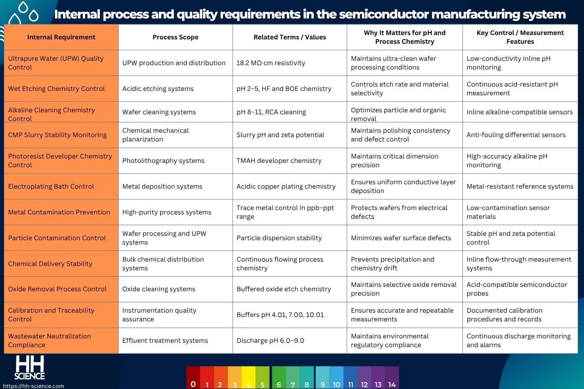
Internal process and quality requirements in the semiconductor manufacturing system
Internal process and quality requirements in semiconductor manufacturing systems define how wafer cleaning chemistry, wet etching precision, CMP slurry stability, ultrapure water (UPW) purity, electroplating consistency, photoresist processing, contamination control, chemical delivery stability, and wastewater neutralization must be continuously monitored and controlled to maintain nanometer-scale fabrication accuracy, low defect density, and high semiconductor yield. These internal requirements establish tightly controlled operating targets for parameters such as pH, resistivity, conductivity, dissolved silica, metal ion contamination, particle concentration, total organic carbon (TOC), slurry dispersion stability, and wastewater discharge chemistry, including conditions such as approximately pH 2–5 for acidic etching systems, pH 8–11 for alkaline cleaning processes, near-neutral UPW systems at 18.2 MΩ·cm, and pH 6.0–9.0 for discharge compliance.
| Internal Requirement | Process Scope | Related Terms / Values | Why It Matters for pH and Process Chemistry | Key Control / Measurement Features |
| Ultrapure Water (UPW) Quality Control | UPW production and distribution | 18.2 MΩ·cm resistivity | Maintains ultra-clean wafer processing conditions | Low-conductivity inline pH monitoring |
| Wet Etching Chemistry Control | Acidic etching systems | pH 2–5, HF and BOE chemistry | Controls etch rate and material selectivity | Continuous acid-resistant pH measurement |
| Alkaline Cleaning Chemistry Control | Wafer cleaning systems | pH 8–11, RCA cleaning | Optimizes particle and organic removal | Inline alkaline-compatible sensors |
| CMP Slurry Stability Monitoring | Chemical mechanical planarization | Slurry pH and zeta potential | Maintains polishing consistency and defect control | Anti-fouling differential sensors |
| Photoresist Developer Chemistry Control | Photolithography systems | TMAH developer chemistry | Maintains critical dimension precision | High-accuracy alkaline pH monitoring |
| Electroplating Bath Control | Metal deposition systems | Acidic copper plating chemistry | Ensures uniform conductive layer deposition | Metal-resistant reference systems |
| Metal Contamination Prevention | High-purity process systems | Trace metal control in ppb–ppt range | Protects wafers from electrical defects | Low-contamination sensor materials |
| Particle Contamination Control | Wafer processing and UPW systems | Particle dispersion stability | Minimizes wafer surface defects | Stable pH and zeta potential control |
| Chemical Delivery Stability | Bulk chemical distribution systems | Continuous flowing process chemistry | Prevents precipitation and chemistry drift | Inline flow-through measurement systems |
| Oxide Removal Process Control | Oxide cleaning systems | Buffered oxide etch chemistry | Maintains selective oxide removal precision | Acid-compatible semiconductor probes |
| Calibration and Traceability Control | Instrumentation quality assurance | Buffers pH 4.01, 7.00, 10.01 | Ensures accurate and repeatable measurements | Documented calibration procedures and records |
| Wastewater Neutralization Compliance | Effluent treatment systems | Discharge pH 6.0–9.0 | Maintains environmental regulatory compliance | Continuous discharge monitoring and alarms |
Compliance-driven monitoring needs in the semiconductor manufacturing system
Compliance-driven monitoring needs in semiconductor manufacturing systems are required to ensure wafer quality, ultrapure water (UPW) purity, contamination control, chemical process stability, worker safety, wastewater discharge compliance, cleanroom integrity, and adherence to semiconductor fabrication specifications under nanometer-scale manufacturing conditions. Continuous monitoring of parameters such as pH, resistivity, conductivity, dissolved silica, total organic carbon (TOC), trace metal contamination, particle concentration, slurry stability, chemical purity, and wastewater chemistry is essential to maintain tightly controlled conditions including approximately pH 2–5 for acidic etching systems, pH 8–11 for alkaline cleaning processes, near-neutral UPW systems with resistivity near 18.2 MΩ·cm, and pH 6.0–9.0 for wastewater discharge, minimizing contamination defects, corrosion, process instability, environmental violations, and semiconductor yield loss.
| Compliance Requirement | Monitoring Scope | Related Terms / Values | Why It Matters for pH and Process Chemistry | Key Measurement / System Features |
| Ultrapure Water (UPW) Compliance | UPW production and distribution systems | 18.2 MΩ·cm resistivity | Maintains ultra-clean semiconductor processing conditions | Low-conductivity inline pH and resistivity monitoring |
| Wet Etching Chemistry Compliance | Acidic etching systems | pH 2–5, HF and BOE chemistry | Controls etch precision and material selectivity | Continuous acid-resistant pH measurement |
| Alkaline Cleaning Process Compliance | Wafer cleaning systems | pH 8–11, RCA cleaning chemistry | Optimizes contamination removal and surface quality | Inline alkaline-compatible sensors |
| CMP Slurry Stability Monitoring | CMP circulation systems | Slurry pH and zeta potential | Maintains polishing consistency and defect control | Anti-fouling differential sensor systems |
| Photoresist Developer Compliance | Photolithography processing | TMAH developer chemistry | Maintains critical dimension precision | High-accuracy alkaline pH monitoring |
| Electroplating Chemistry Compliance | Metal deposition systems | Acidic copper plating chemistry | Ensures uniform conductive layer formation | Metal-resistant reference systems |
| Trace Metal Contamination Monitoring | High-purity chemical systems | ppb–ppt contamination levels | Protects wafers from electrical defects | Low-contamination sensor materials |
| Particle Contamination Control | Wafer processing and UPW systems | Particle dispersion stability | Minimizes wafer surface contamination defects | Stable pH and zeta potential management |
| Chemical Delivery Stability Monitoring | Bulk chemical distribution systems | Continuous flowing process chemistry | Prevents precipitation and chemistry drift | Inline flow-through monitoring systems |
| Oxide Removal Process Compliance | Oxide cleaning systems | Buffered oxide etch chemistry | Maintains selective oxide removal accuracy | Acid-compatible semiconductor probes |
| Calibration and Traceability Compliance | Instrumentation quality assurance | Buffers pH 4.01, 7.00, 10.01 | Ensures accurate and auditable measurements | Documented calibration and SCADA logging |
| Wastewater Discharge Compliance | Effluent treatment and discharge | Discharge pH 6.0–9.0 | Maintains environmental regulatory compliance | Continuous neutralization and discharge monitoring |
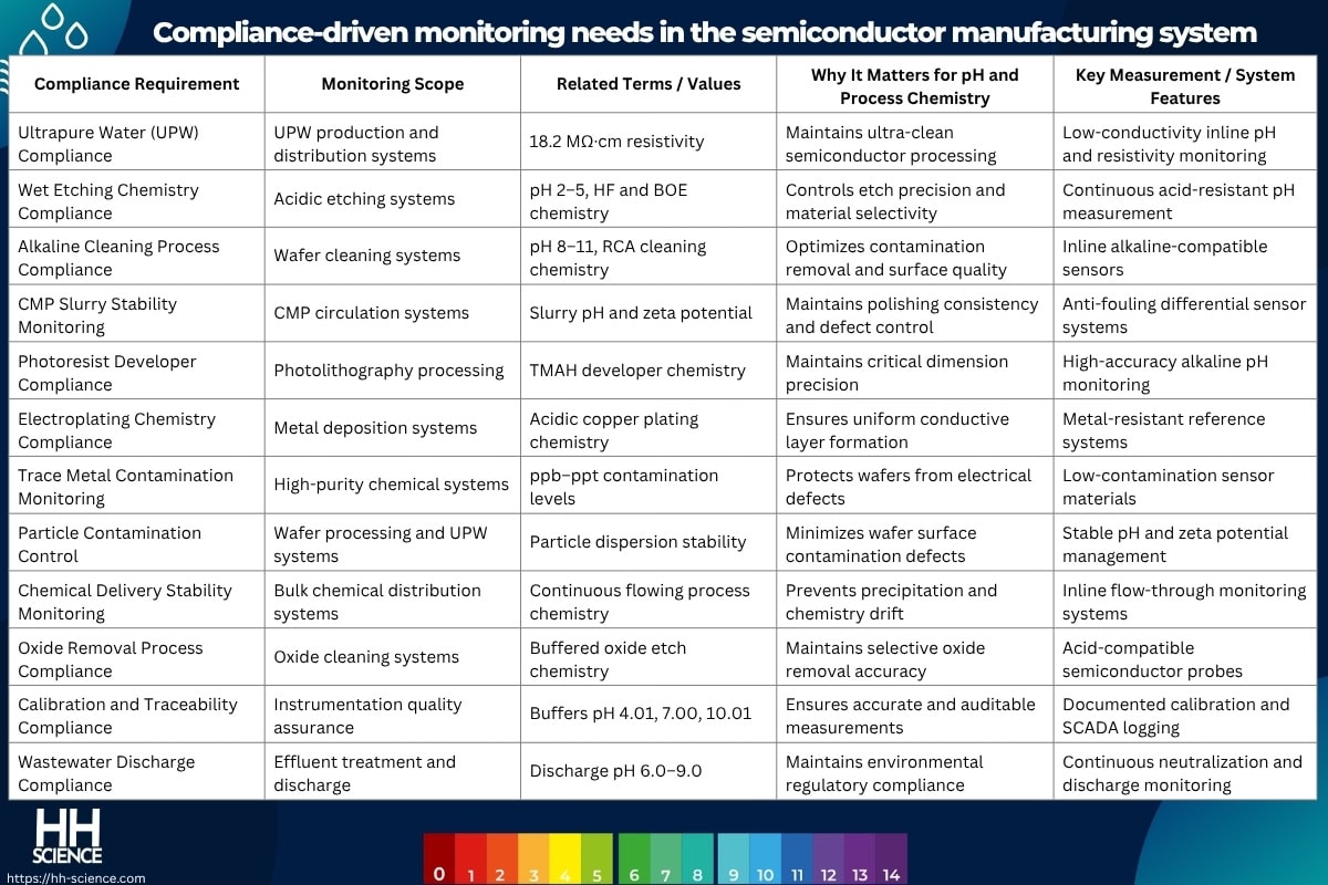
Selecting the right pH measurement approach in a semiconductor manufacturing system
Selecting the right pH measurement approach in semiconductor manufacturing systems is critical because applications such as ultrapure water (UPW) production, wet etching, alkaline wafer cleaning, CMP slurry circulation, electroplating, photoresist development, chemical delivery, oxide removal, and wastewater neutralization involve ultra-low conductivity conditions near 18.2 MΩ·cm, aggressive acidic and alkaline chemistries, particle-loaded slurries, trace metal contamination sensitivity in the ppb–ppt range, temperature-sensitive reactions, and nanometer-scale process tolerances where even minor measurement drift can affect wafer yield and device reliability. Choosing appropriate technologies—such as low-conductivity combination sensors, differential or double-junction reference systems, semiconductor-grade low-metal-contamination materials, digital smart sensors with automatic temperature compensation (ATC), anti-fouling flow-through assemblies, chemically resistant glass membranes, and inline or immersion installation designs—ensures highly stable measurement accuracy (typically ±0.01–0.05 pH), reliable contamination control, stable chemical selectivity, reduced maintenance frequency, improved process repeatability, and compliance with semiconductor process specifications including approximately pH 2–5 for etching systems, pH 8–11 for cleaning processes, and pH 6.0–9.0 for wastewater discharge.
Decision support for the semiconductor manufacturing system
Decision support in semiconductor manufacturing systems evaluates factors such as ultrapure water (UPW) resistivity near 18.2 MΩ·cm, process chemistry type, contamination sensitivity in the ppb–ppt range, slurry particle loading, operating temperature, flow conditions, metal ion exposure, wafer material compatibility, and wastewater discharge limits (pH 6.0–9.0) to determine the most suitable pH measurement solution for each fabrication process. By analyzing process-specific requirements—including approximately pH 2–5 for acidic etching systems, pH 8–11 for alkaline cleaning processes, CMP slurry chemistry stability, and electroplating bath control—decision support helps semiconductor engineers and process specialists select the proper sensor technology, installation method, calibration strategy, and maintenance interval needed to maintain stable wafer processing, low defect density, and high semiconductor yield.
Application-driven measurement strategies
Application-driven measurement strategies align pH monitoring technologies with specific semiconductor process conditions such as UPW production, wet etching, wafer cleaning, CMP slurry circulation, electroplating, photolithography, chemical blending, oxide removal, and wastewater neutralization, each having unique conductivity, contamination, temperature, and chemical compatibility requirements. These strategies determine whether low-conductivity sensors, differential reference systems, anti-fouling designs, semiconductor-grade low-metal-contamination materials, inline flow-through assemblies, immersion probes, or digital smart sensors with automatic temperature compensation (ATC) are required to maintain highly stable pH measurement, minimize contamination risk, improve process repeatability, and reduce maintenance frequency in contamination-sensitive semiconductor fabrication environments.
Linking semiconductor manufacturing systems to sensor selection and OEM solutions
Linking semiconductor manufacturing systems to sensor selection and OEM solutions ensures that pH instrumentation is specifically engineered for aggressive semiconductor chemistries, ultra-pure process conditions, abrasive CMP slurries, trace contamination sensitivity, continuous inline monitoring, and nanometer-scale fabrication tolerances. OEM solutions typically combine semiconductor-grade low-contamination materials, low-conductivity pH sensors, differential or double-junction reference systems, anti-fouling flow cells, automatic temperature compensation (ATC), digital communication protocols (Modbus, HART, Ethernet), and PLC/SCADA integration to provide highly stable measurement accuracy (typically ±0.01–0.05 pH), improved contamination control, predictive diagnostics, reliable process automation, and long-term semiconductor manufacturing stability.


